

Home NewsHard and Flexible: New Palladium-Based Alloy Will Simplify Testing of Microelectronic Equipment
Hard and Flexible: New Palladium-Based Alloy Will Simplify Testing of Microelectronic Equipment
Published January 12 - 2025
The Japanese company TANAKA has unveiled its latest innovation—TK-SK, a new palladium-based alloy designed for manufacturing probe pins (Probe Pins) used in the final stages of printed circuit board (PCB) testing. This advanced material was presented at the SWTest Asia 2024 conference held on October 24–25, 2024, in Fukuoka Prefecture, Japan. Initial samples of products made from the TK-SK alloy will be available by the end of the year. With this innovative development, TANAKA aims to boost its electronic components sales by 1.5 times within the next three years.
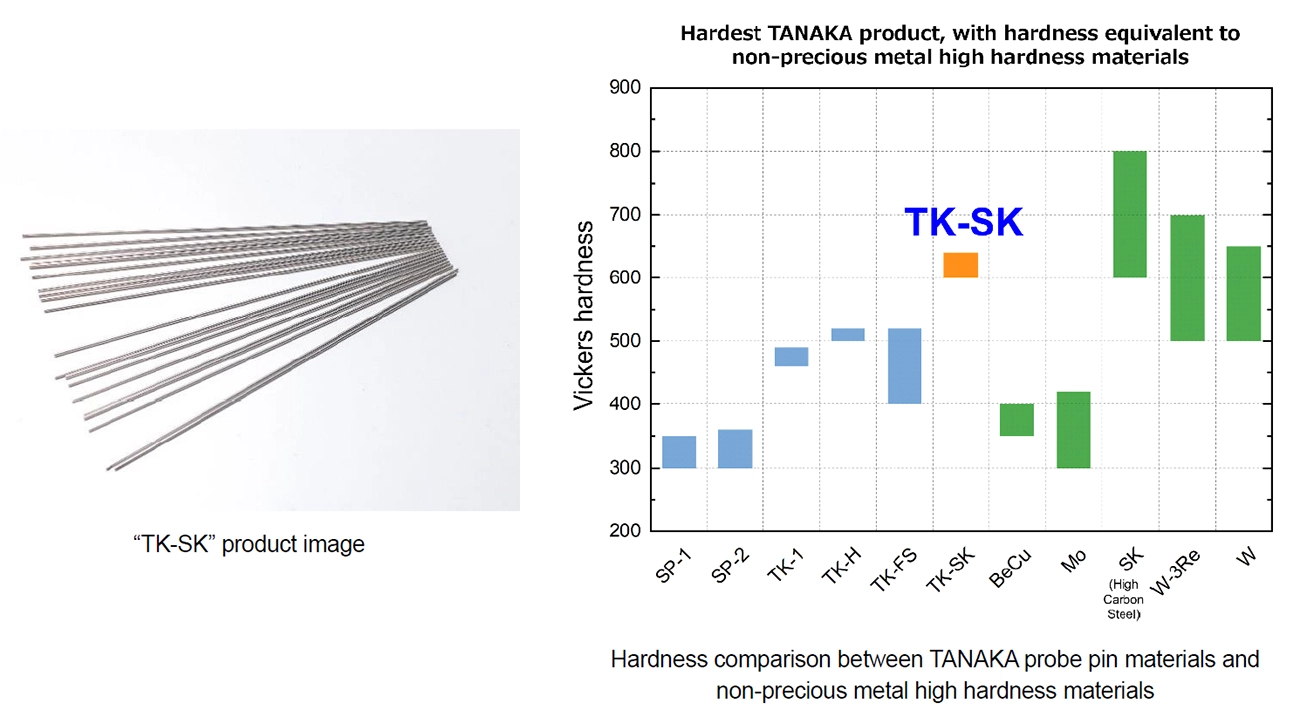
The TK-SK alloy boasts an impressive hardness rating of 640 HV (HV means Vickers hardness, see box). This places it at the forefront of the electronic testing connectors market. While TANAKA offers around ten different alloys for manufacturing probe pins, most exhibit hardness levels ranging between 300–400 HV, with a few reaching 500–550 HV. The maximum previously achievable hardness was 560 HV, making TK-SK the hardest alloy in the company’s portfolio.
Vickers hardness (HV) is measured by pressing a diamond pyramid with a 136° apex angle into the surface of the material. The resulting indentation, usually a diamond-shaped mark, is used to calculate the hardness based on the diagonals of the imprint. The Vickers method is versatile, applicable to both surface layers and thin sheet materials. Standard testing parameters include a load of up to 100 kgf and a hold time of 10–15 seconds. Practical HV measurement ranges from 145 to 1000 HV.
By developing a high-hardness alloy, TANAKA has achieved a significant milestone in materials science. The exceptional hardness of TK-SK ensures that probe pins retain their shape, delivering reliable and stable contact with tested objects—essential for precise electrical parameter measurements in semiconductors.
A unique feature of TK-SK is its bending resistance. Probe pins made from this alloy withstand up to ten repeated bends (based on TANAKA’s internal standards) without breaking. This combination of extreme hardness and flexibility is unprecedented, as hard materials are typically brittle.
The alloy’s composition includes 48.9% palladium and 19.25% silver, along with copper and other metals. The addition of silver and copper enhances flexibility and electrical conductivity while maintaining exceptional wear resistance.
The introduction of TK-SK paves the way for creating precise, thin, and lightweight probe pin designs, expanding testing possibilities for smaller circuit boards. This innovation is crucial for modern microelectronics, where each new generation of devices is more compact than the last.
The high hardness of TK-SK also addresses a common issue with Pogo pin contact probes: wear and deformation. During frequent use, these pins are prone to damage from friction and solder adhesion, necessitating regular maintenance.
How are the Pogo pins used?
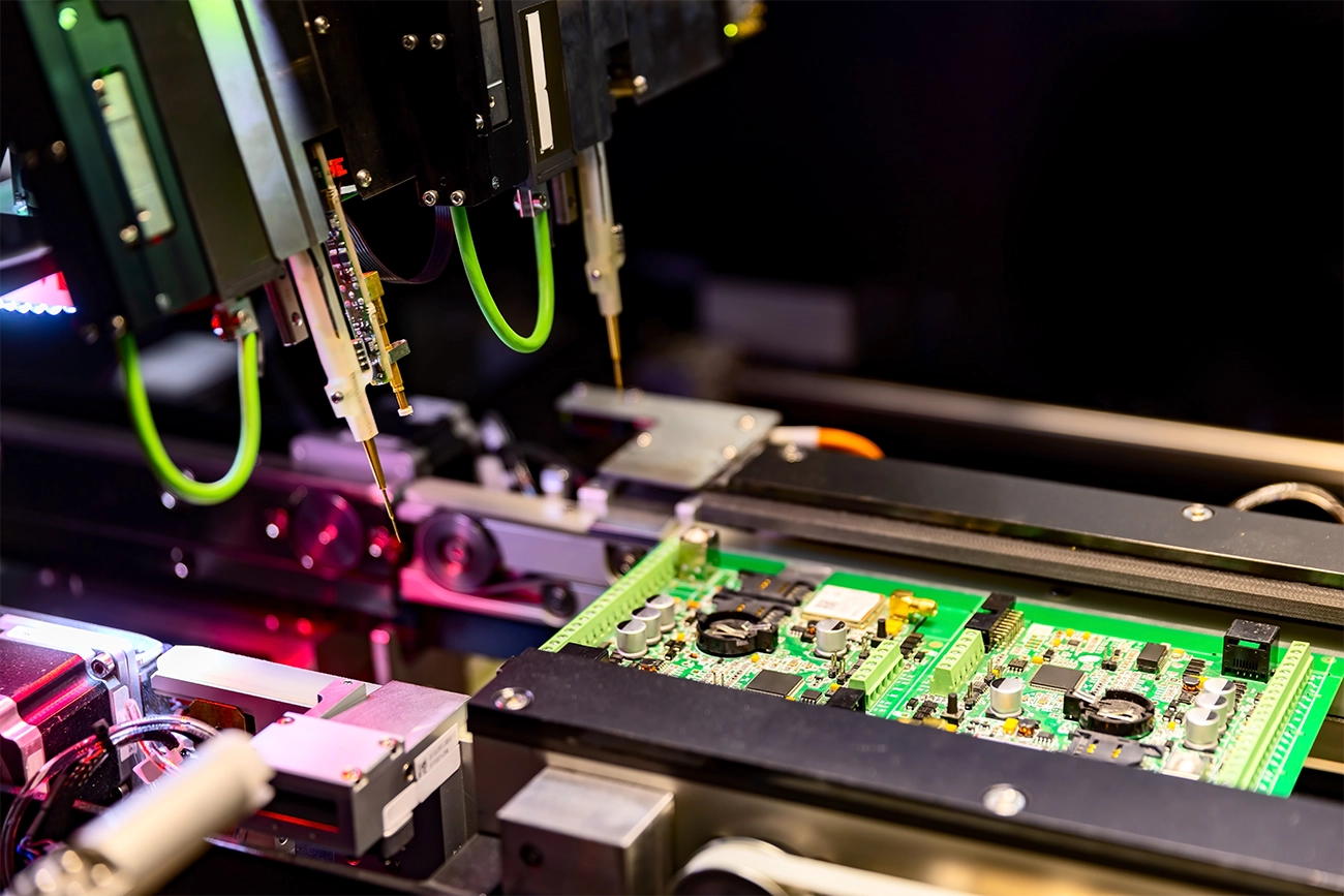
The process of manufacturing printed circuit boards and final electronic devices involves several stages of testing the equipment as it goes through the assembly process: from checking the performance of each specific element to the functioning of the entire assembled printed circuit board. For this purpose, the developers leave special contact points during the PCB design process, where it is possible to apply voltage and measure the result and determine whether the created assembly works on the device, thus finding out whether the PCB is correctly assembled.
Testing is typically conducted in the final assembly stage using specialized devices like “bed-of-nails” fixtures, which rely on pogo pins. While numerous alloys are available for pogo pins, precious metal-based alloys are preferred for their superior conductivity, albeit at a higher cost. This makes wear resistance a critical requirement. The new TK-SK alloy promises to set a new standard for durability in test equipment.

Pogo pins During Circuit Board Testing by a Bed of Nails
The remarkable wear resistance of TK-SK not only extends the lifespan of contact probes but also reduces the maintenance costs of expensive testing equipment. This alloy is poised to play a pivotal role in the semiconductor industry’s transition to a new technological paradigm. While currently positioned as a material for probe pins, the TK-SK alloy is expected to be adapted for a broader range of applications in the coming years, similar to the trajectory of TANAKA’s previous flagship palladium alloy, TK-FS (Vickers hardness: 400–520 HV).
Palladium Base of Contacts in Microelectronics
Materials with a hardness of 640 HV are not new to humanity. High-carbon and alloy steels, ceramics, and carbide-based materials have long been used in tooling and mechanical components. These materials are wear-resistant and maintain their shape under heavy mechanical loads.
However, such materials—especially steels with high electrical resistance or non-conductive ceramics—are unsuitable for electronics. The TK-SK alloy’s palladium base enables a unique combination of mechanical durability, excellent conductivity (≤7.0 μΩ·cm), and chemical stability.
Few metals, even precious ones, are suitable for manufacture of strong, flexible and current-conductive materials. Copper, silver and gold have the perfect electrical conductivity but they are very soft, and connections and contacts made of these metals are easily worn. This is why engineers use palladium as the base for microelectronic devices. The combination of resistance to corrosion, high melting point and electrical conductivity makes it perfect for conductors and ensures reliable and efficient connections within the printed circuit boards and between them. At the same time, palladium is hard and has lower density which means that 1 milligram of the metal takes up a volume larger than, for example, 1 milligram of gold.
Out of TANAKA’s ten palladium-based alloys for microelectronics contacts, six have palladium contents ranging from 33% to 56%. These alloys include other metals such as gold, platinum, silver, and copper, making them solderable and versatile for various applications
Palladium is also used to alloy other materials, such as semiconductor contact pads. This enables the creation of thin, high-quality metal layers that improve electrical performance and contact stability—crucial for high-frequency and high-speed circuits.
The Secret Bureau
The demand for high-hardness sensor pins has been growing recently; but as the hardness increases, material processing becomes even harder due to equipment breaking during cutting, for example. This is why creation of a new alloy is not enough – a procedure is needed for its processing and for manufacture of products unique in terms of accuracy and subtlety.
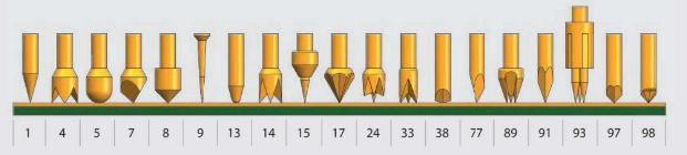
Fig. Different Pogo Pins Used for Electronic Equipment Testing
For example, producing TK-SK probe pins requires ultra-thin wire (≤0.5 mm) from the alloy, which demands cutting-edge equipment capable of withstanding the alloy’s hardness. Processes such as cutting and polishing must meet microscopic precision standards, as pogo pins are tiny components with exacting requirements.
Few companies worldwide possess the expertise, technology, and tools necessary to achieve this—TANAKA is one of them.
Founded in 1885, TANAKA began as a currency exchange enterprise before shifting focus to precious metals for industrial applications. Over nearly 140 years, the company has become a leader in precious metal processing, particularly platinum group metals. TANAKA’s expertise attracted the Japanese military during the early 20th century, steering the company toward strategic technologies.
Today, TANAKA Holdings Co. comprises over 20 companies operating in Japan and internationally (India, Taiwan, China, and the USA), employing over 5,000 people. Its product range spans from bonding wires to nanostructured catalysts for fuel cells, serving industries such as electronics, semiconductors, automotive, aerospace, telecommunications, pharmaceuticals, and glass manufacturing. In fiscal 2023, TANAKA’s group sales exceeded USD 4 billion.
Source: https://tanaka-preciousmetals.com/en/news_release/20241017/
Recent News
October 09 - 2025
Ivanhoe Mines, a Canadian mining and exploration company known for several high-profile discoveries, has driven underground development into the high-grade Platreef orebody for the first time. The company’s Executive Co-Chair Robert Friedland and President and Chief Executive Officer Marna Cloete detailed the breakthrough, with mining crews entering the orebody at the 850-metre level with the first blast of high-grade ore in early May.

September 24 - 2025
Canadian exploration company Power Metallic has reported results from its deepest intersection to date at the Lion Zone, carried out in the wake of successful exploration activities last year. The 2024 discovery of the zone, 5.5 kilometres away from the Nisk Main Zone, has shifted the company’s focus towards what could prove a game-changing discovery.

September 05 - 2025
Australian mining company Southern Palladium has received an environmental authorization (EA) on its flagship Tier 1 Bengwenyama project from South Africa’s Department of Mineral and Petroleum Resources (DMPR). The license outlines rights on underground mining and related infrastructural activities on the project, marking a key milestone towards development.

August 25 - 2025
A study from a team of chemists working at McGill University in Montreal, Canada has proposed a new method for synthesising palladium catalysts using electrochemical potential, supporting both oxidative addition and reductive elimination with two-electron exchange in mild temperature and pressure conditions.

August 05 - 2025
A team of functional materials researchers in China developed a copper–palladium catalyst that has been shown to improve catalytic activity and selectivity in the electrochemical nitrate reduction reaction (NO3RR), leading to improved ammonia yields. Scaling this process could significantly reduce the energy and environmental burden of the ammonia industry as a whole.

July 21 - 2025
Zhe Gong et al. from the China University of Geosciences and Zhiping Deng and Xiaolei Wang from the University of Alberta (Canada) have developed a highly efficient palladium catalyst that could support the large-scale rollout of hydrogen fuel cells. The catalyst was designed by doping palladium with cobalt producing atomic cobalt (Co)-doped Pd metallene (Co-Pdene), and demonstrated exceptional electrocatalytic performance while maintaining its structural integrity.